

The NPN transistor is one of the most fundamental and widely used electronic components in modern circuitry. It serves as both an amplifier and a switch, making it an essential part of almost every electronic device — from radios and computers to communication systems and power regulators. In semiconductor technology, the NPN transistor is a type of Bipolar Junction Transistor (BJT) that uses electrons as the majority charge carriers, which makes it faster and more efficient than its PNP counterpart.
What is an NPN Transistor?
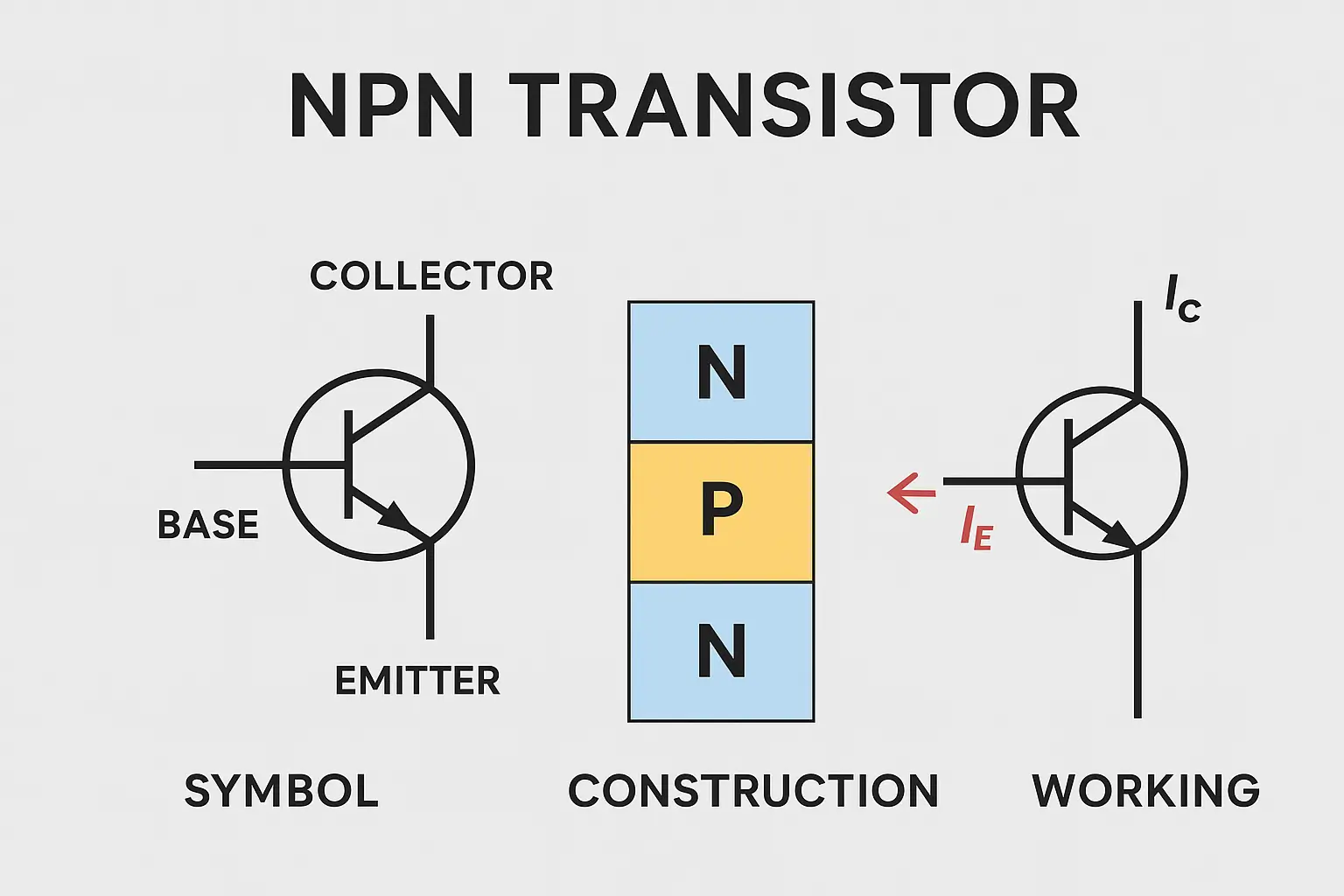
An NPN transistor is a three-layer, three-terminal semiconductor device that consists of two n-type materials separated by a thin layer of p-type material. It is called “NPN” because of this specific arrangement of semiconductor layers — Negative-Positive-Negative.
In this configuration, the emitter (E) and collector (C) are made of n-type semiconductor material, while the base (B) is a thin p-type region sandwiched between them. When properly biased, the NPN transistor allows electrons to flow easily from the emitter to the collector, enabling current amplification and switching functions.
According to Morris Mano (Digital Design Expert), “The ability of a small input current to control a larger output current is what makes the transistor the heart of modern electronics.”
Construction of NPN Transistor
The construction of an NPN transistor involves three main regions, each performing a distinct role in the device’s operation:
- Emitter (E): The emitter is heavily doped to inject a large number of free electrons into the base region.
- Base (B): The base is very thin and lightly doped, allowing most electrons from the emitter to pass through to the collector.
- Collector (C): The collector is moderately doped and larger in size to collect the electrons from the base region and dissipate heat effectively.
The transistor is enclosed in a casing (metal or plastic) with three terminals corresponding to the emitter, base, and collector. The NPN transistor symbol features an arrow pointing outward on the emitter leg, representing the direction of conventional current flow (from base to emitter).
Working of NPN Transistor
The working of an NPN transistor is based on charge carrier movement and junction biasing. It has two p-n junctions — the emitter-base junction (EBJ) and the collector-base junction (CBJ) — whose biasing determines transistor behavior.
Active Mode Operation
In the active region, the emitter-base junction is forward-biased, and the collector-base junction is reverse-biased. A small base current controls a much larger collector current, creating amplification.
When a positive voltage is applied to the base relative to the emitter, electrons from the emitter move into the base region. Since the base is thin and lightly doped, most of these electrons cross into the collector region.
This results in:
- Base current (IB) – small control current
- Collector current (IC) – large output current
- Emitter current (IE) – total current (sum of IB and IC)
Mathematically,
IE = IB + IC
and the current gain (β) is defined as:
β = IC / IB
Typical current gain values for NPN transistors range from 20 to 1000, depending on the transistor’s type and material.
Cutoff and Saturation Regions
In the cutoff region, both junctions are reverse-biased, and the transistor behaves like an open switch — no current flows through the device.
In the saturation region, both junctions are forward-biased, allowing maximum current flow; the transistor behaves like a closed switch.
This dual behavior enables NPN transistors to function as electronic switches in logic circuits, microcontrollers, and digital systems.
Applications of NPN Transistor
NPN transistors are among the most commonly used transistors in electronics because of their superior switching speed, high current gain, and ease of control. Some key applications include:
Amplification
NPN transistors are widely used as signal amplifiers in audio, radio, and communication devices. They can amplify small input voltages to much larger output voltages while maintaining signal integrity.
Switching Circuits
They act as solid-state switches in logic circuits, microcontrollers, and power regulators. When the base voltage is high, the transistor conducts (ON state), and when the base voltage is zero, it remains off (OFF state).
Oscillators and Modulators
Used in frequency generation and modulation circuits, NPN transistors help produce stable oscillations in radio transmitters and receivers.
Current Control
They regulate current flow in various devices, including sensors, relays, and automated control systems, by controlling a large load current through a small base current.
Computers and Processors
NPN transistors are fundamental elements in logic gates, amplifying circuits, and integrated circuits (ICs), forming the foundation of modern computing devices.
Advantages of NPN Transistors
NPN transistors are favored over PNP transistors in most designs because electrons, the majority carriers in NPNs, move faster than holes. This results in:
- Higher efficiency and faster switching speeds
- Better current handling capability
- Simpler biasing with a positive voltage supply
- Compatibility with TTL and CMOS logic families
Conclusion
The NPN transistor remains a cornerstone of modern electronics due to its versatility, speed, and efficiency. From acting as a reliable amplifier to serving as a high-speed digital switch, it plays a vital role in powering and controlling electronic systems. Understanding its construction, working, and applications not only provides a strong foundation for electrical engineering students but also enhances the design capability of professionals in electronics and automation fields.
Most Popular NPN Transistors and Their Specifications
| Transistor Model | Max Voltage (VCE) | Max Current (IC) | Power Dissipation (PD) | Current Gain (hFE) | Package Type | Common Applications | Special Features |
|---|---|---|---|---|---|---|---|
| 2N2222A | 40V | 800 mA | 500 mW | 75–30 | TO-18 | Signal amplification, RF circuits | Fast switching, low noise |
| BC547 | 45V | 100 mA | 500 mW | 110–800 | TO-92 | Audio amplifiers, sensors | Low leakage, stable operation |
| 2N3904 | 40V | 200 mA | 625 mW | 100–300 | TO-92 | General-purpose switching | High speed, low VCE(sat) |
| BD139 | 80V | 1.5 A | 12.5 W | 25–250 | TO-126 | Power amplifiers, drivers | High current, medium power |
| TIP31C | 100V | 3 A | 40 W | 10–50 | TO-220 | Power switching, audio amps | High power, robust design |
| 2N3055 | 60V | 15 A | 115 W | 20–70 | TO-3 | Regulators, inverters | Excellent thermal stability |
| BC337 | 45V | 800 mA | 625 mW | 100–630 | TO-92 | LED drivers, control circuits | High gain, reliable switching |
| 2N1711 | 50V | 500 mA | 800 mW | 40–120 | TO-39 | RF and audio circuits | High frequency response |
Frequently Asked Questions (FAQ)
1. What is an NPN transistor used for?
An NPN transistor is used for switching and amplification in electronic circuits. It controls large current flow through the collector using a small current at the base, making it essential in devices like amplifiers, logic circuits, and microcontrollers.
2. How does an NPN transistor work?
An NPN transistor works when a small base current allows a larger current to flow from the collector to the emitter. The emitter-base junction is forward-biased, and the collector-base junction is reverse-biased, enabling electron movement and current amplification.
3. What is the symbol of an NPN transistor?
The symbol of an NPN transistor has an arrow pointing outward on the emitter leg, indicating the direction of conventional current flow (from base to emitter). The three terminals are labeled as Emitter (E), Base (B), and Collector (C).
4. What are the differences between NPN and PNP transistors?
The NPN transistor uses electrons as majority carriers, while the PNP transistor uses holes. NPN transistors conduct when the base is positive relative to the emitter, whereas PNP transistors conduct when the base is negative relative to the emitter.
5. Why is an NPN transistor preferred over a PNP transistor?
NPN transistors are preferred because electrons move faster than holes, resulting in higher efficiency, faster switching speed, and simpler circuit design with a positive power supply. They are also more common in modern electronic applications.
6. What is the current gain (β) in an NPN transistor?
The current gain (β) is the ratio of the collector current (IC) to the base current (IB). It determines how effectively the transistor amplifies the current. Typical β values range from 20 to 1000, depending on the transistor type.
7. Can an NPN transistor be used as a switch?
Yes. In switching applications, when the base current is applied, the transistor goes into saturation mode (ON state), allowing full current through the collector. When no base current is applied, it enters cutoff mode (OFF state), stopping current flow.
8. What materials are used to make NPN transistors?
NPN transistors are made using silicon (Si) or gallium arsenide (GaAs) as semiconductor materials. Silicon-based transistors are more common because of their stability, cost-effectiveness, and thermal performance.
Author’s comment
So friends, I’m Pralay Bhunia, I hope I’ve been able to help you with this information about NPN Transistor (BJT). If you have any more questions or suggestions, please feel free to share them in the comments. Your support always inspires me to share more new information.
External link
- Npn Transistor – an overview | ScienceDirect